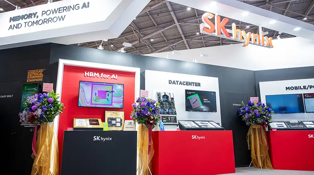
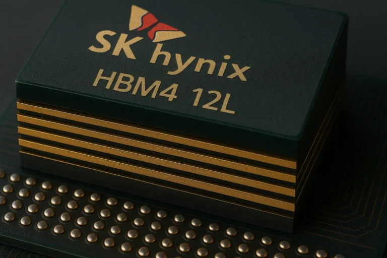
Seoul In a move that felt equal parts product launch and mic-drop, SK hynix this week lifted the lid on its 12-layer HBM4 package, a 36-gigabyte vertical slab of silicon that can sling north of two terabytes of data every second. The South Korean chipmaker quietly shipped engineering samples to “major customers” back on March 19, but only started parading the part in public last month at Computex Taipei, where a plexiglass case surrounding the memory stack drew an almost comic-book glow of smartphone flashes.
The headline figures border on sci-fi: a per-package bandwidth of 2 TB/s—roughly 400 full-HD movies per second—and 60 percent more throughput than HBM3E, the part Nvidia’s current Blackwell GPUs are guzzling. SK hynix credits an “Advanced MR-MUF” molding process that stops the 12-high tower from warping while also acting as a heat spreader, something early HBM3E engineers lost hair over.
“We have enhanced our position as a front-runner in the AI ecosystem after years of grinding through the physics,” Justin Kim, president of the company’s AI Infrastructure business, said when the samples began flying out the door. “We’re now ready to cruise through performance certification and into mass production.” Kim sounded relaxed, but sources at the company hint the certification sprint is more of a marathon—customer qualification cycles for HBM4 are running longer than HBM3E simply because the stack is that much denser.

Still, the vibe at the SK hynix booth in Taipei’s Nangang Exhibition Center was downright cocky. Under a slogan reading “Memory, Powering AI and Tomorrow,” the firm parked its 12-layer HBM4 next to a live demo of 12-high HBM3E wired to Nvidia’s GB200 board. Visitors had to queue just to snap a photo. Company reps, perhaps sensing the optics, cheekily taped an empty space beside the display with a sign: “16-layer HBM4—see you in ’26.”
Analysts aren’t blinking. TrendForce notes that SK hynix is already the exclusive supplier of 12-high HBM3E for Nvidia’s Blackwell Ultra GPUs and is now positioned to funnel HBM4 into the next-gen Rubin accelerator family slated for a late-2025 debut. The same research house projects that HBM will swallow more than 30 percent of DRAM market value next year, a startling climb from under 10 percent just two years ago.
Rivals are scrambling. Micron finished a 12-stack HBM3E last September but hasn’t yet snagged a marquee design win, while Samsung is still chasing validation for its own 12-high parts. “Explosive” is the word SK hynix CEO Kwak Noh-jung recently used to describe demand as he told shareholders that 2026’s entire HBM output could be sold before a single wafer hits the slicer.
Beyond the speed-freak numbers, engineers are whispering about the less-sexy bits: skew-tolerant TSVs, a beefed-up base die that finally keeps I/O pins under control, and power-saving tricks that cut watt-per-bit by “double-digit percentages,” according to one slide the company half-heartedly tried to keep under wraps in Taipei. Those optimizations matter because AI data-center operators are starting to sweat their power budgets almost as much as their capex.
Assuming the certification slog stays on track, SK hynix aims to flip the switch on volume production in the second half of 2025. If that timeline holds—and if Nvidia’s Rubin boards land as scheduled—next year’s flagship GPUs could ship with nearly 300 GB/s more memory bandwidth than the current champs. In an AI market that seems to move faster than anyone’s crystal ball, that extra headroom might be the difference between merely training a large language model and teaching it to write its own stand-up routine. Either way, SK hynix has made it painfully clear: the HBM arms race is no longer about who reaches the summit, but about who can keep adding floors to the skyscraper.
